R&D
Overview
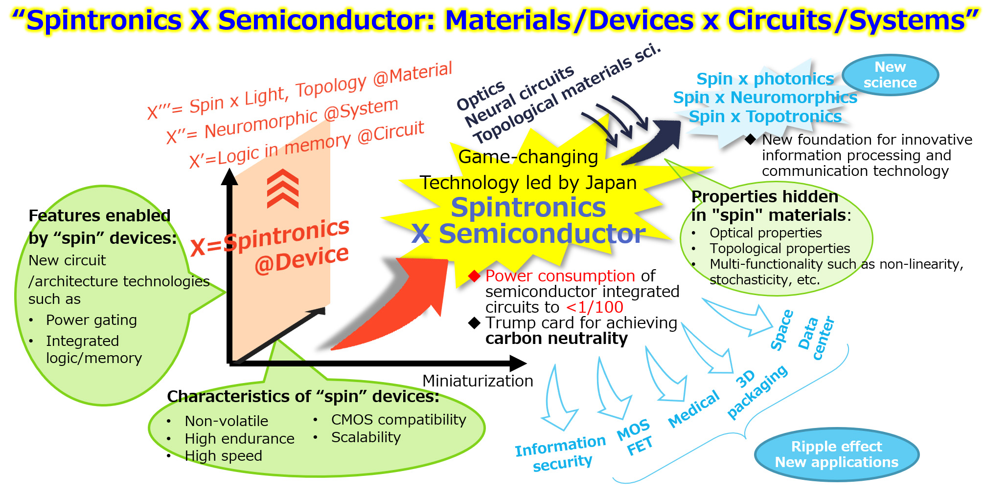
At this hub, we will promote a series of semiconductor research and development from materials and devices to integrated processes, circuits, architectures, chips and systems, with “spintronics” as the new approach (X). We study the physical properties and functionality unexplored in spintronic materials, and open new fields such as spin x photonics, spin x neuromorphics, and spin x topotronics that will serve as new foundations for innovative information processing and communication technologies. The established insights will be applied for realizing new-concept computing as well as creating a new technological platform for various applications such as MOSFETs, 3D packaging, medical care, information security, and space data centers.
R&D Scope
R&D for various new materials/devices as well as circuits/architectures taking advantage of materials/devices’ characteristics, enabled by spintronics as a new approach X for high-performance semiconductor.
⇒Globally competitive research areas supported by robust academic and technological foundations of Japan’s strengths and synergies between the two fields
R&D Scheme
- Promoting with three layers from materials to integration:
- Widely drive basic research (participation of a wide variety of researchers) in the basic/fundamental research layer (bottom) to create new scientificfrontiers and develop new applications
- Promising technologies are transferred to the single device demonstration layer (middle) and integration demonstration layer (upper), and prototype verification
- Collaborative private companies survey market research, specifications, exit strategies, killer apps, and support research and development for social implementation
